• The Computer Microchip: Modern microchips descend from integrated circuits used in the Apollo Guidance Computer.
• Light-Emitting Diodes (LED): Developed by NASA,the red light-emitting diodes were used to grow plants in space. Later this technology was developed in medical devices for muscle pain relief/relaxation, joint pain, arthritis and muscle spasms. Later generations of the technology are used to combat the symptoms of bone atrophy, multiple sclerosis, diabetic complications and Parkinson's disease.
LAOROSA DESIGN-JUNKY 26 NASA Inventions That We Take For Granted Everyday...
Once again you should not use junk web sites .....................
[Excerpt]
Background
Electroluminescence, the natural phenomena upon which LED technology is built was discovered in 1907 by British radio researcher and assistant to
Guglielmo Marconi , Henry Joseph Round, while experimenting with silicon carbide and a cats whisker.
During the 1920s, Russian radio researcher Oleg Vladimirovich Losev was studying the phenomena of electroluminescence in the diodes used in radio sets. In 1927, he published a paper called
Luminous carborundum [silicon carbide] detector and detection with crystals about his research, and while no practical LED was created at that time based on his work, his research did influence future inventors.
Years later in 1961, Robert Biard and Gary Pittman invented and patented an infrared LED for Texas instruments. This was the first LED, however, being infrared it was beyond the visible light spectrum. Humans can not see infrared light. Ironically, Baird and Pittman only accidentally invented a light emitting diode while the pair were actually attempting to invent a laser diode.
Visible LEDs
In 1962, Nick Holonyack, a consulting engineer for General Electric Company, invented the first visible light LED. It was a red LED and Holonyack had used gallium arsenide phosphide as a substrate for the diode.
Holonyack has earned the honor of being called the "Father of the light emitting diode" for his contribution to the technology. He also holds 41 patents and his other inventions include the laser diode and the first light dimmer. (Another interesting fact about Holonyack was that he was once the student of
John Bardeen, the co-inventor of the
transistor.)
In 1972, electrical engineer, M George Craford invented the first yellow colored LED for the Monsanto Company using gallium arsenide phosphide in the diode. Craford also invented a red LED that was 10 times brighter than Holonyack's.
It should be noted that the Monsanto Company was the first to mass-produce visible LEDs. In 1968, Monsanto produced red LEDs used as indicators. But it was not until the 1970s that LEDs became popular, when Fairchild Optoelectronics began producing low-cost LED devices (less than five cents each) for manufacturers.
In 1976, Thomas P. Pearsall invented a high-efficiency and extremely bright LED for use in fiber optics and fiber telecommunications. Pearsall invented new semiconductor materials optimized for optical fiber transmission wavelengths.
In 1994, Shuji Nakamura invented the first blue LED using gallium nitride.
[Excerpt]
Who Invented LED or the Light Emitting Diode
• The Computer Microchip: Modern microchips descend from integrated circuits used in the Apollo Guidance Computer.
.
Comprehension is the word of the day, the way that reads is ....................
[Excerpt]
Integrated circuit
From Wikipedia, the free encyclopedia
(Redirected from
Microchip)
"Silicon chip" redirects here. For the electronics magazine, see
Silicon Chip.
"Microchip" redirects here. For other uses, see
Microchip (disambiguation).

Erasable programmable read-only memory integrated circuits. These
packages have a transparent window that shows the
die inside. The window allows the memory to be erased by exposing the chip to
ultraviolet light.
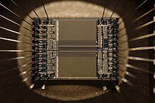
Integrated circuit from an
EPROM memory microchip showing the memory blocks, the supporting circuitry and the fine silver wires which connect the integrated circuit die to the legs of the packaging.
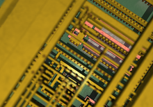
Synthetic detail of an integrated circuit through four layers of planarized copper interconnect, down to the polysilicon (pink), wells (greyish), and substrate (green)
An
integrated circuit or
monolithic integrated circuit (also referred to as an
IC, a
chip, or a
microchip) is a set of
electronic circuits on one small plate ("chip") of
semiconductor material, normally
silicon. This can be made much smaller than a
discrete circuit made from independent components. ICs can be made very compact, having up to several billion
transistors and other
electronic components in an area the size of a fingernail. The width of each conducting line in a circuit can be made smaller and smaller as the technology advances; in 2008 it dropped below 100
nanometer,
[1] and now it is tens of nanometers.
[2]
ICs were made possible by experimental discoveries showing that
semiconductor devices could perform the functions of
vacuum tubes and by mid-20th-century technology advancements in
semiconductor device fabrication. The integration of large numbers of tiny
transistors into a small chip was an enormous improvement over the manual assembly of circuits using discrete
electronic components. The integrated circuit's
mass production capability, reliability, and building-block approach to
circuit design ensured the rapid adoption of standardized integrated circuits in place of designs using discrete transistors.
There are two main advantages of ICs over
discrete circuits: cost and performance. Cost is low because the chips, with all their components, are printed as a unit by
photolithography rather than being constructed one transistor at a time. Furthermore, much less material is used to construct a packaged IC die than to construct a discrete circuit. Performance is high because the components switch quickly and consume little power (compared to their discrete counterparts) as a result of the small size and close proximity of the components. As of 2012, typical chip areas range from a few square millimeters to around 450 mm2, with up to 9 million
transistors per mm2.
Integrated circuits are used in virtually all electronic equipment today and have revolutionized the world of
electronics.
Computers,
mobile phones, and other digital
home appliances are now inextricable parts of the structure of modern societies, made possible by the low cost of producing integrated circuits.
Invention
Main article:
Invention of the integrated circuit
Early developments of the integrated circuit go back to 1949, when the German engineer
Werner Jacobi (
Siemens AG)
[6] filed a patent for an integrated-circuit-like semiconductor amplifying device
[7] showing five transistors on a common substrate in a 3-stage
amplifier arrangement. Jacobi disclosed small and cheap
hearing aids as typical industrial applications of his patent. An immediate commercial use of his patent has not been reported.
The idea of the integrated circuit was conceived by a radar scientist working for the
Royal Radar Establishment of the British
Ministry of Defence,
Geoffrey W.A. Dummer (1909–2002). Dummer presented the idea to the public at the Symposium on Progress in Quality Electronic Components in
Washington, D.C. on 7 May 1952.
[8] He gave many symposia publicly to propagate his ideas, and unsuccessfully attempted to build such a circuit in 1956.
A precursor idea to the IC was to create small ceramic squares (wafers), each one containing a single miniaturized component. Components could then be integrated and wired into a bidimensional or tridimensional compact grid. This idea, which looked very promising in 1957, was proposed to the US Army by
Jack Kilby, and led to the short-lived Micromodule Program (similar to 1951's
Project Tinkertoy).
[9] However, as the project was gaining momentum, Kilby came up with a new, revolutionary design: the IC.
 Jack Kilby
's original integrated circuit
Newly employed by
Texas Instruments, Kilby recorded his initial ideas concerning the integrated circuit in July 1958, successfully demonstrating the first working integrated example on 12 September 1958.
[10] In his patent application of 6 February 1959,
[11] Kilby described his new device as “a body of semiconductor material … wherein all the components of the electronic circuit are completely integrated.”
[12] The first customer for the new invention was the
US Air Force.
[13]
Kilby won the 2000 Nobel Prize in Physics for his part of the invention of the integrated circuit.
[14] Kilby's work was named an
IEEE Milestone in 2009.
[15]
Noyce also came up with his own idea of an integrated circuit half a year later than Kilby. His chip solved many practical problems that Kilby's had not. Produced at
Fairchild Semiconductor, it was made of
silicon, whereas Kilby's chip was made of
germanium.
Robert Noyce credited
Kurt Lehovec of
Sprague Electric for the
principle of p–n junction isolation caused by the action of a biased p–n junction (the diode) as a key concept behind the IC.
[16]
Fairchild Semiconductor was also home of the first silicon-gate IC technology with
self-aligned gates, which stands as the basis of all modern
CMOS computer chips. The technology was developed by Italian physicist
Federico Faggin in 1968, who later joined Intel in order to develop the very first Central Processing Unit (CPU) on one chip (
Intel 4004), for which he received the
National Medal of Technology and Innovation in 2010.
Generations
In the early days of integrated circuits, only a few transistors could be placed on a chip, as the scale used was large because of the contemporary technology, and manufacturing yields were low by today's standards. As the degree of integration was small, the design process was relatively simple. Over time, millions, and today billions,
[17] of transistors could be placed on one chip, and a good design required thorough planning. This gave rise to new
design methods.
SSI, MSI and LSI
The first integrated circuits contained only a few transistors. Called "small-scale integration" (SSI), digital circuits containing transistors numbering in the tens provided a few logic gates for example, while early linear ICs such as the
Plessey SL201 or the
Philips TAA320 had as few as two transistors. The term Large Scale Integration was first used by
IBM scientist
Rolf Landauer when describing the theoretical concept[
citation needed], from there came the terms for SSI, MSI, VLSI, and ULSI.
SSI circuits were crucial to early aerospace projects, and aerospace projects helped inspire development of the technology. Both the Minuteman missile and Apollo program needed lightweight digital computers for their inertial guidance systems; the Apollo guidance computer led and motivated the integrated-circuit technology,[18] while the Minuteman missile forced it into mass-production. The Minuteman missile program and various other Navy programs accounted for the total $4 million integrated circuit market in 1962, and by 1968, U.S. Government space and defense spending still accounted for 37% of the $312 million total production. The demand by the U.S. Government supported the nascent integrated circuit market until costs fell enough to allow firms to penetrate the industrial and eventually the consumer markets. The average price per integrated circuit dropped from $50.00 in 1962 to $2.33 in 1968.[19] Integrated circuits began to appear in consumer products by the turn of the decade, a typical application being FM inter-carrier sound processing in television receivers.
The next step in the development of integrated circuits, taken in the late 1960s, introduced devices which contained hundreds of transistors on each chip, called "medium-scale integration" (MSI).
They were attractive economically because while they cost little more to produce than SSI devices, they allowed more complex systems to be produced using smaller circuit boards, less assembly work (because of fewer separate components), and a number of other advantages.
Further development, driven by the same economic factors, led to "large-scale integration" (LSI) in the mid-1970s, with tens of thousands of transistors per chip.
Integrated circuits such as 1K-bit RAMs, calculator chips, and the first microprocessors, that began to be manufactured in moderate quantities in the early 1970s, had under 4000 transistors. True LSI circuits, approaching 10,000 transistors, began to be produced around 1974, for computer main memories and second-generation microprocessors.
VLSI
Main article:
Very-large-scale integration

Upper interconnect layers on an
Intel 80486DX2 microprocessor die
The final step in the development process, starting in the 1980s and continuing through the present, was "very large-scale integration" (
VLSI). The development started with hundreds of thousands of transistors in the early 1980s, and continues beyond several billion transistors as of 2009.
Multiple developments were required to achieve this increased density. Manufacturers moved to smaller design rules and cleaner fabrication facilities, so that they could make chips with more transistors and maintain adequate yield. The path of process improvements was summarized by the
International Technology Roadmap for Semiconductors (ITRS).
Design tools improved enough to make it practical to finish these designs in a reasonable time. The more energy efficient
CMOS replaced
NMOS and
PMOS, avoiding a prohibitive increase in power consumption.
In 1986 the first one megabit
RAM chips were introduced, which contained more than one million transistors. Microprocessor chips passed the million transistor mark in 1989 and the billion transistor mark in 2005.
[20] The trend continues largely unabated, with chips introduced in 2007 containing tens of billions of memory transistors.
[21]
ULSI, WSI, SOC and 3D-IC
To reflect further growth of the complexity, the term
ULSI that stands for "ultra-large-scale integration" was proposed for chips of complexity of more than 1 million transistors.
[22]
Wafer-scale integration (WSI) is a system of building very-large integrated circuits that uses an entire silicon wafer to produce a single "super-chip". Through a combination of large size and reduced packaging, WSI could lead to dramatically reduced costs for some systems, notably massively parallel supercomputers. The name is taken from the term Very-Large-Scale Integration, the current state of the art when WSI was being developed.
[23]
A
system-on-a-chip (SoC or SOC) is an integrated circuit in which all the components needed for a computer or other system are included on a single chip. The design of such a device can be complex and costly, and building disparate components on a single piece of silicon may compromise the efficiency of some elements. However, these drawbacks are offset by lower manufacturing and assembly costs and by a greatly reduced power budget: because signals among the components are kept on-die, much less power is required (see
Packaging).
[24]
A
three-dimensional integrated circuit (3D-IC) has two or more layers of active electronic components that are integrated both vertically and horizontally into a single circuit. Communication between layers uses on-die signaling, so power consumption is much lower than in equivalent separate circuits. Judicious use of short vertical wires can substantially reduce overall wire length for faster operation.
[25][/Excerpt]
Now we have beat around and around that bush and you have come up empty every time, the source you site is a hack and I have volumes more research to disprove it ......................
In the highlighted section the phrase "led and motivated" does not mean invented !!


